

News

Science
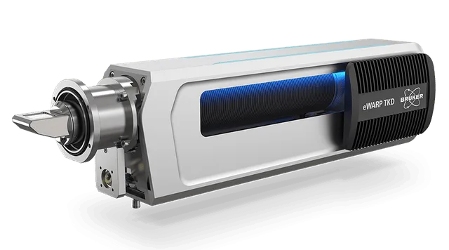
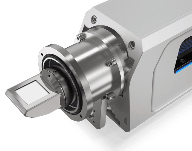
eWARP TKD is the latest addition to the award-winning eWARP family of detectors, powered by Bruker’s cutting-edge Wide ARea Pixelated (WARP) sensor technology, and designed specifically for Transmission Kikuchi Diffraction (TKD).
With eWARP our unique WARP sensors began a new era of EBSD with ultra-fast mapping speeds at unprecedented spatial resolution and more. Leveraging the same breakthrough WARP technology, eWARP TKD is redefining the limits of TKD (also known as Transmission EBSD), opening new possibilities for high-resolution nanomaterial analysis.
At the core of the system is a newly developed pixelated sensor with 162 × 162 pixels and an active area exceeding 26 × 26 mm2.
eWARP TKD is purpose-built for nanomaterials characterization using the "on-axis" sample-detector geometry in the Scanning Electron Microscope (SEM). eWARP TKD outperforms existing solutions across all key metrics, with unmatched sensitivity, speed, spatial resolution and data integrity.
eWARP TKD is a detector for our QUANTAX EBSD analytical system.
eWARP TKD redefines nanomaterials characterization in the SEM, delivering a powerful set of advantages for researchers and engineers working on nanomaterials:
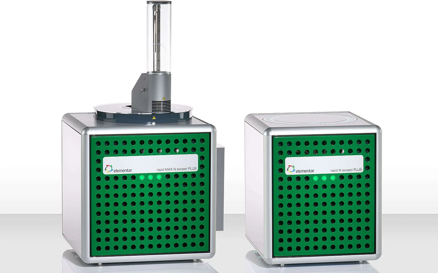
New nitrogen and protein analyzers of the exceed PLUS series...
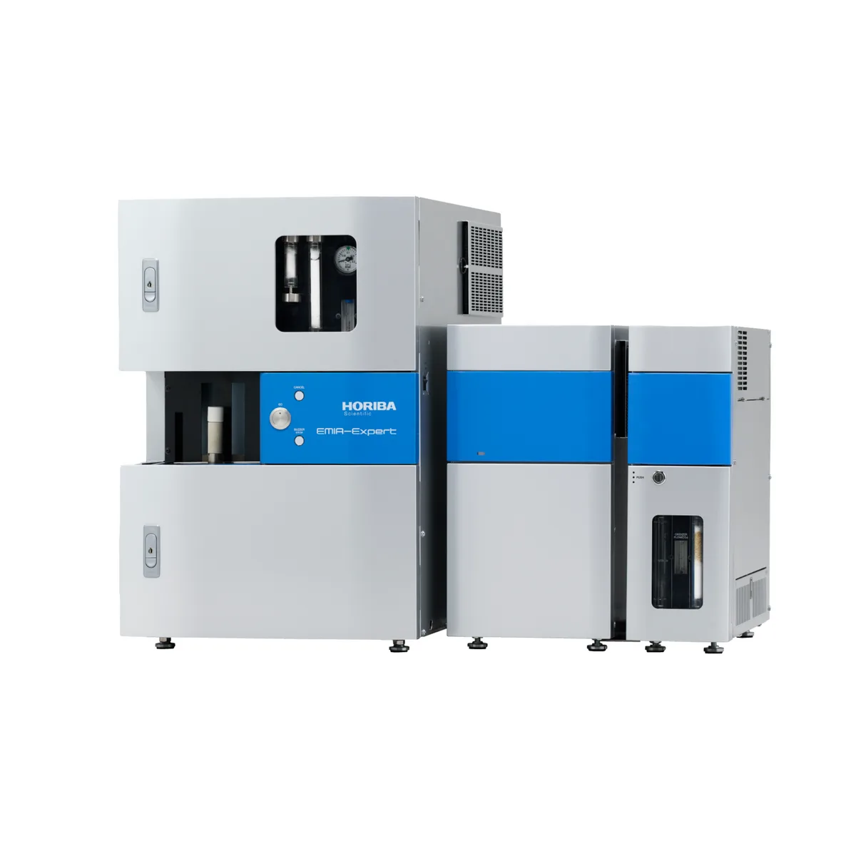
Highly repeatable carbon analysis of high-carbon materials to support R&D and stable manufacturing processes
EDS Webinar The Future of EDS Starts Here - Introducing inclined 4-Channel Detection